Reverse Engineering the Anelace BCD Clock
Introduction

It all began with a birthday present. The Anelace BCD clock was a nice addition to my desk, just the flickering of the LEDs representing the seconds was a bit distracting. I thought there is almost certainly just a microcontroller inside, so how hard could it be to change the programming a bit?
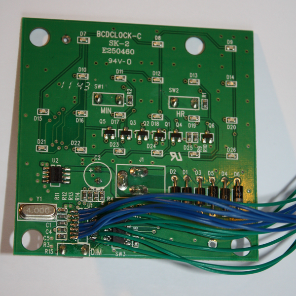
Opening the case was easy, the PCB was easy to remove. The main components are a PIC 16F505 microcontroller, a 4051 decoder, some diodes, some LEDs, a voltage regulator and some buttons.
After some research the plan was to buy a PICkit2 for which a command line utility was available in source code. That had a chance to work on my preferred platform (OpenBSD). Some PIC utilities like assembler and linker were available already as part of the gputils package. The microntroller was available in the same SO-14 package like used in the clock through Reichelt for less than 1€. With that, I could read out the microcontroller, do some modifications and reprogram it. An maybe even test with a second microntroller before destroying the original one.
As it was not clear to me whether it's OK to connect up the programmer to the PIC while being connected to the circuit, I desoldered the microcontroller and put it on a breakout board, just to be safe.
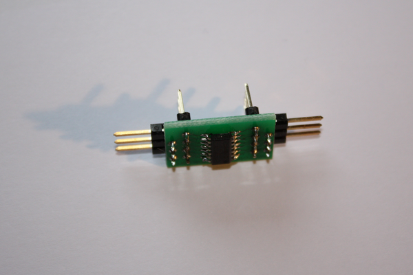
The breakout could easily be connected to the PICkit 2 so that I could read out the program memory. This is what I got:
000000:  0064  clrf	0x4
000001:  0a20  goto	0x20
000002:  0fff  xorlw	0xff
000003:  0fff  xorlw	0xff
000004:  0fff  xorlw	0xff
000005:  0fff  xorlw	0xff
000006:  01e2  addwf	0x2, f
000007:  080c  retlw	0xc
000008:  0802  retlw	0x2
000009:  0805  retlw	0x5
00000a:  080c  retlw	0xc
00000b:  0066  clrf	0x6
00000c:  0067  clrf	0x7
00000d:  0c2c  movlw	0x2c
00000e:  0006  tris	0x6
00000f:  007a  clrf	0x1a
000010:  0787  btfss	0x7, 0x4
000011:  051a  bsf	0x1a, 0
000012:  07a7  btfss	0x7, 0x5
000013:  053a  bsf	0x1a, 0x1
000014:  0646  btfsc	0x6, 0x2
000015:  055a  bsf	0x1a, 0x2
000016:  0ce8  movlw	0xe8
000017:  0006  tris	0x6
000018:  0066  clrf	0x6
000019:  0800  retlw	0
00001a:  0fff  xorlw	0xff
00001b:  0fff  xorlw	0xff
00001c:  0fff  xorlw	0xff
00001d:  0fff  xorlw	0xff
00001e:  0fff  xorlw	0xff
00001f:  0fff  xorlw	0xff
000020:  0cd7  movlw	0xd7
000021:  0002  option
000022:  0c06  movlw	0x6
000023:  0024  movwf	0x4
000024:  0060  clrf	0
000025:  02a4  incf	0x4, f
000026:  07a4  btfss	0x4, 0x5
000027:  0a24  goto	0x24
000028:  0070  clrf	0x10
000029:  0064  clrf	0x4
00002a:  0c19  movlw	0x19
00002b:  0030  movwf	0x10
00002c:  0031  movwf	0x11
00002d:  0c30  movlw	0x30
00002e:  0007  tris	0x7
00002f:  090b  call	0xb
000030:  0c3c  movlw	0x3c
000031:  0028  movwf	0x8
000032:  0c41  movlw	0x41
000033:  0038  movwf	0x18
000034:  0c03  movlw	0x3
000035:  003f  movwf	0x1f
000036:  0aab  goto	0xab
000037:  0201  movf	0x1, w
000038:  003c  movwf	0x1c
000039:  00fc  decf	0x1c, f
00003a:  0004  clrwdt
00003b:  0caa  movlw	0xaa
00003c:  003d  movwf	0x1d
00003d:  020a  movf	0xa, w
00003e:  0e08  andlw	0x8
00003f:  0029  movwf	0x9
000040:  0000  nop
...
0003fe:  0000  nop
0003ff:  0c26  movlw	0x26
000400:  000f  dw	0xf  ;unknown opcode
000401:  000f  dw	0xf  ;unknown opcode
000402:  000f  dw	0xf  ;unknown opcode
000403:  000f  dw	0xf  ;unknown opcode
000fff:  0fc9  xorlw	0xc9
So there is some code that looks like real code, but most parts are missing. This is where I found there is a code protection facility inside the PIC, which is enabled. It causes only the 64 bytes to be readable, the rest of the program memory is zeroed out. Circumventing the code protection might be possible, but it's certainly not easy. I decided to not go down that path, instead I was going to learn how to program PIC and rewrite the firmware from scratch.
Tracing the circuit
To know how to program the BCD clock I first needed to understand the circuit better. Since the PIC was desoldered already and placed on a breakout board, it was pretty easy to follow the connections and draw the schematics with gschem. Here is the result (klick to enlarge):
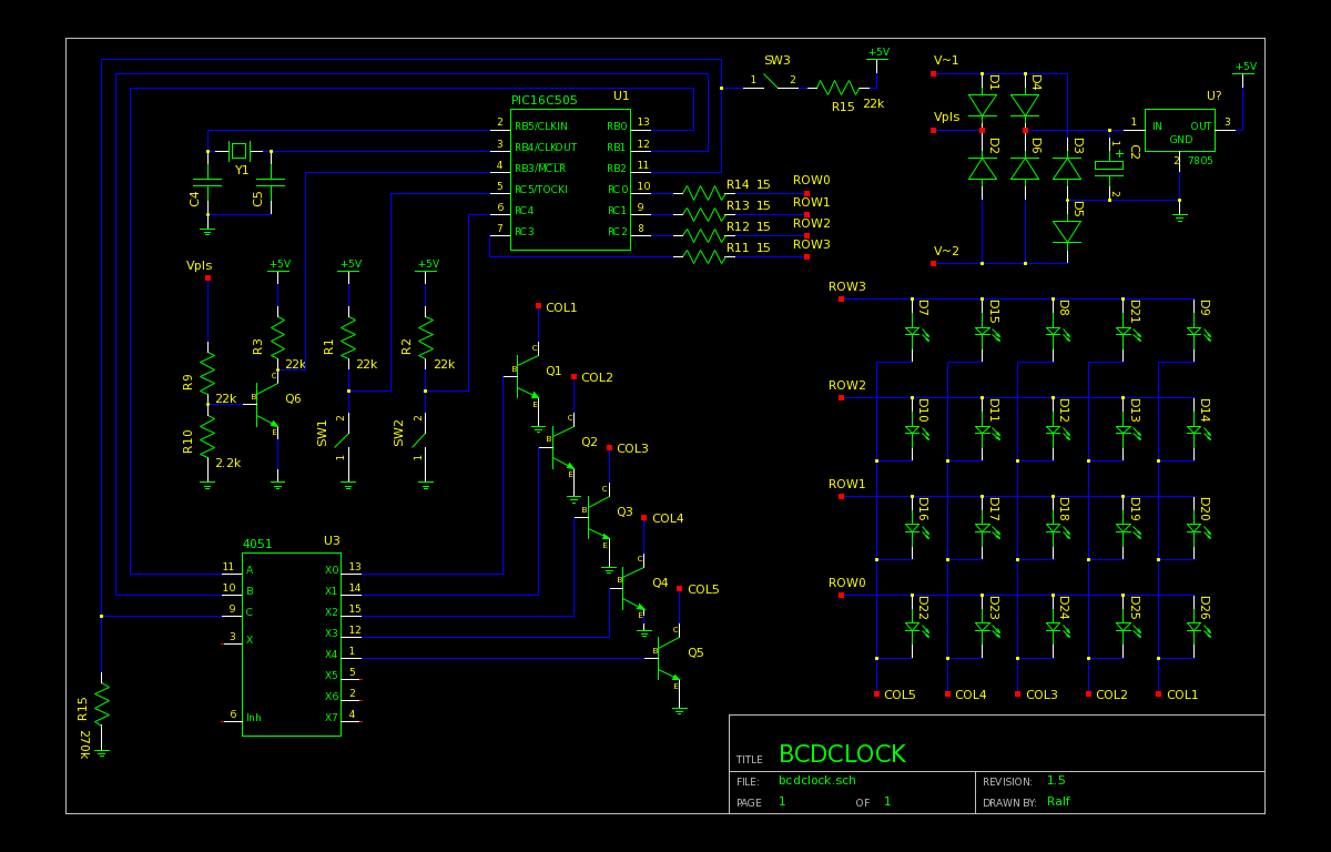
There is a standard bridge rectifier connected to a 7805 voltage regulator to generate 5V. The two additional diodes D1 and D2 create 100Hz positive sine pulses that get fed into transistor Q6 which would invert and amplify the signal to nearly rectangular pulses with 100 Hz. Some research turned up that the AC frequency of the power network at least in Europe is accurate enough to use it for driving clocks, so this was likely the purpose for feeding that signal into the microcontroller.
The rest is pretty straight forward. RB0 to RB2 are used to drive the 4051 which would enable the different columns of the LED matrix. RC0 to RC3 would drive the rows. Please note that D15 and D21 are physically located in the leftmost column to represent the second digit of the hour.
For the input buttons, RC3 and RC4 are used to hook up the switches labeled HR and MIN that are used to set the time in the original firmware. SW3 controls the brightness of the LEDs. It reuses RB2, which is used for both reading SW3 and driving the 4051.
Simulation environment
For rewriting the complete firmware it occurred to me that it would be pretty useful to simulate the microcontroller in software and ideally simulate the peripherals as well. Fortunately there is gpsim, a free software simulator for a wide variety PIC controllers. Unfortunately gpsim didn't support the 16F505 initially. But it was quite easy to extend, so I added support for the 16F505. The patch has been provided to the gpsim project (Update 2014-11-20: 16F505 support has been included in gpsim-0.28).
Gpsim has a way to connect some simple peripherals like buttons, LEDs and simple logic gates to the controller. That would have been sufficient already to implement the 4051 gate and driving the LEDs by emulating the row/column selection with AND gates driving the resistors. Since implementing a logic component in gpsim is pretty straightforward, I instead added a 4051-like component and used that for the simulation.
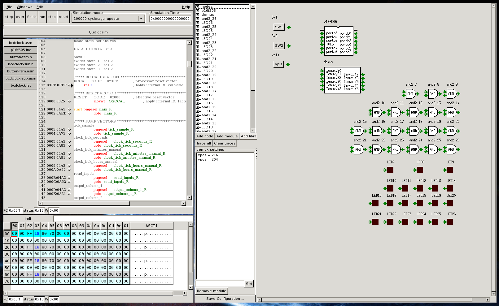
Please note that I didn't add all the simulation components via the GUI. The netlist format is pretty straightforward, so most of LEDs and AND gates are actually generated with a script. Also, SW3 is not implemented. But that setup was good enough to start with coding.
As you need to understand more or less every bit of the microcontroller in order to write a correct simulator, in hindsight it was a good way to learn how to program the 16F505.
Programming environment
Research didn't turn up any free software C compiler that would support both the target microcontroller 16F505 and OpenBSD. But there is gputils available which includes an assembler and disassembler with support for 16F505. So this was the tool of choice. I could write assembly code and test the first parts in the simulation environment, which was enough to implement the basic clock functionality.
Testing on the real device
As I was not quite sure whether I could program the PIC while being connected to the rest of the circuit (although from the schematics it looked like it's possible), I came up with a setup that let me easily connect either the programmer or the circuit. For that I soldered wires to the microcontroller pads on the PCB to connect it to a breadboard.
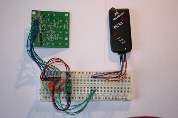
This way I could connect the programmer with some jumper wires in a straightforward way and disconnect the PCB if necessary. Turned out that the PCB didn't have to be disconnected, programming can be done in circuit. Only when powering the controller with the power supply the programmer needs to be disconnected.
The final version has the 16F505 soldered on the board again with a 5 pin header soldered with some wires on top of the microcontroller pins, so that programming is still possible without too much effort.
Usage
The original firmare uses several combination of buttons to switch between various modes, like 12/24 hours, bcd or real binary clock mode. My firmware uses a different approach. There are no button combinations. There are two modes:
- clock display mode
- configure mode
SW3 is used to toggle between clock mode and configure mode. In clock display mode, SW1 and SW2 can be used to set the time.
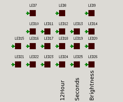
In configure mode, SW1 cycles to the various settings while SW2 changes it. The current selected setting is blinking. SW2 cycles through the possible options. E.g. for brightness, there are 4 levels which are indicated by the number of LEDs in the settings columns. At the same time, the brightness is immediately changed for all LEDs.
It's probably easier to try it out than to describe it.
Conclusion
The whole process took about 3 months and it was certainly a lot of fun. Many thanks to Julia for this nice present, which she actually expected to be the most boring one.
Links
- https://github.com/ra1fh/bcdclock - The BCD clock code
- http://gputils.sourceforge.net/ - GNU PIC utilities
- http://gpsim.sourceforge.net/ - PIC microcontroller simulator